Canon’s cost-effective nano-imprinting lithography offers semiconductor innovation but faces potential trade curbs to China, driven by U.S. pressure. The technology aims to challenge ASML’s dominance, making advanced chip production more accessible. However, uncertainties arise due to Japan’s export restrictions and geopolitical tensions. Meanwhile, Japan and Micron invest in domestic chip manufacturing, responding to global supply chain disruptions. These developments set the stage for an evolving semiconductor landscape, with trade barriers and technology innovations at the forefront.
In a significant move within the semiconductor industry, Canon recently unveiled its plans to manufacture nano-imprinting lithography machines, offering a more cost-effective alternative to the existing technology. However, this promising development is likely to be hampered by trade restrictions imposed on China. Canon’s innovation in nano-imprinting lithography (NIL) technology aims to provide a lower-cost option compared to ASML’s chip-making technology. While this could potentially empower smaller manufacturers to produce cutting-edge semiconductors, the looming specter of trade sanctions on China, driven by pressure from the United States, poses a significant challenge.
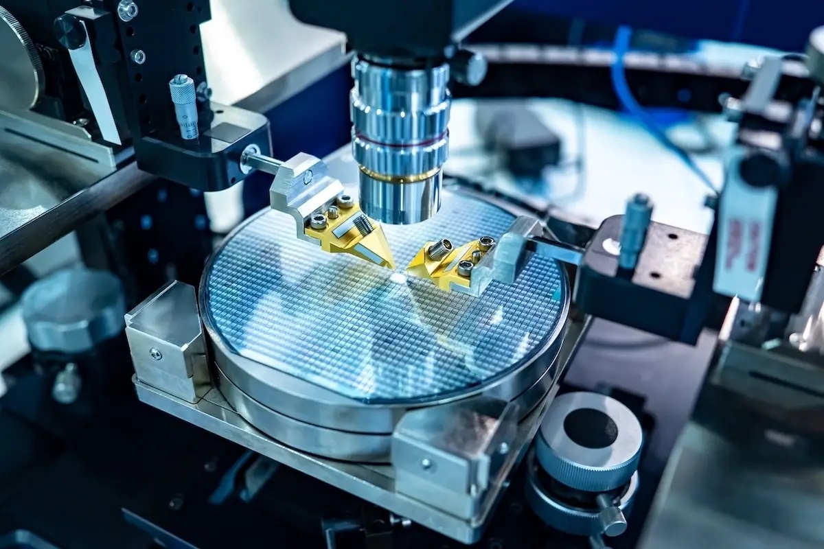
Nano-imprinting lithography, an alternative to ultraviolet (EUV) and deep ultraviolet (DUV) photolithography technology has gained attention as a potential solution for advanced semiconductor device fabrication. Currently, ASML, a Netherlands-based company, stands as the sole supplier of EUV and DUV technology, offering the most advanced chip-making machines used for mass-producing chips smaller than 7nm. However, the exorbitant cost of EUV machines, running into hundreds of millions of dollars, renders this technology inaccessible to many smaller players in the chip market.
To make matters more complex, similar to other chip manufacturers, ASML is barred from exporting its EUV technology to Chinese customers due to US sanctions. The geopolitical tensions surrounding technology exports and the global semiconductor supply chain have contributed to this restrictive environment.
Canon’s announcement last month revealed its intent to launch a nano-imprint lithography (NIL) machine capable of producing parts as small as 5nm nodes, with future potential for 2nm nodes as the technology continues to evolve. This cutting-edge technology diverges from traditional photolithography equipment, which transfers a circuit pattern by projecting it onto the resist-coated wafer. In contrast, Canon’s approach involves pressing a mask imprinted with the circuit pattern onto the wafer’s resist, akin to using a stamp. By eliminating the need for the optical mechanism found in the traditional manufacturing process, Canon anticipates a significant reduction in the cost of machine ownership.
Canon’s CEO, Fujio Mitarai, expressed confidence in their ability to offer this innovative technology at a price point significantly lower than ASML’s EUV machines. Although specific pricing details have not been finalized, Mitarai’s statement hinted at a potentially game-changing cost advantage for Canon’s technology. However, Canon refrained from providing a timeframe for when these machines would be available, leaving the industry eagerly awaiting their debut.
The backdrop of export curbs imposed by the Japanese government, prompted by pressure from the United States to enact trade restrictions on China, further complicates Canon’s ambitions. Notably, these curbs do not explicitly mention nano-imprint technology. Mitarai, the CEO of Canon, clarified that his understanding of Japanese export sanctions implies that exports beyond 14nm technology are prohibited. This interpretation implies that Canon would be unable to sell its innovative technology to China under the existing trade restrictions.
In response to a shifting global landscape driven by supply chain disruptions caused by the COVID-19 pandemic and the US-China tech trade war, numerous countries have intensified their efforts to develop domestic semiconductor manufacturing capabilities. Japan, for instance, pledged a substantial $532 million (70 billion yen) in April 2023 for projects aimed at developing and producing next-generation chips within the country. This included a partnership with Rapidus to manufacture 2nm chips in Japan by 2025.
In May, Micron made a groundbreaking announcement, revealing its intention to invest up to 500 billion yen ($3.6 billion) in bringing extreme ultraviolet lithography (EUV) technology to Japan. This marked the first instance of a company introducing this production method to Japan. Micron’s strategic plans revolve around utilizing these machines to produce the next generation of dynamic random access memory (DRAM), also known as 1-gamma chips, at its Hiroshima plant. DRAM chips are widely utilized in digital electronics, where low-cost and high-capacity memory are essential.
Overall, Canon’s foray into affordable nano-imprinting lithography presents a promising alternative for semiconductor manufacturing, potentially making advanced technology more accessible to smaller players in the industry. However, the cloud of trade restrictions on China casts a shadow of uncertainty on the technology’s prospects in the global market. The delicate balance between technological innovation and geopolitical considerations continues to shape the semiconductor landscape, with nations like Japan and companies like Micron making significant investments to bolster their domestic chip industries. The outcome of these dynamics will undoubtedly influence the future of semiconductor technology and global supply chains.